032025 — 2026
Flight Computer PCB
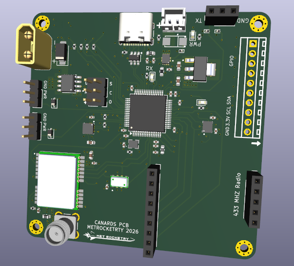
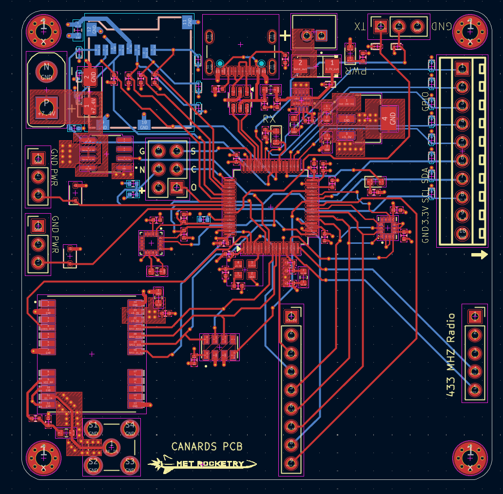
The board the flight software runs on: four layers on a 1.6 mm stackup, MCU in the middle, GPS module and antenna port bottom left, USB-C and servo power along the top, and the radio on a header at the right.
- Where
- MetRocketry Design Team
- Stack
- KiCad, STM32F446, u-blox NEO-M9N, RFM69HCW
- Built with
- Ranvir Singh — shared avionics design work
- 4layers
- 50 ± 5 ΩRF feed
- 2.5 mmSDIO length match
The schematic
Four layers, with dedicated power and ground planes in the middle rather than copper poured between signals. A continuous reference plane under every signal layer keeps return currents short and predictable, which is the cheapest EMI mitigation available on a board this dense.
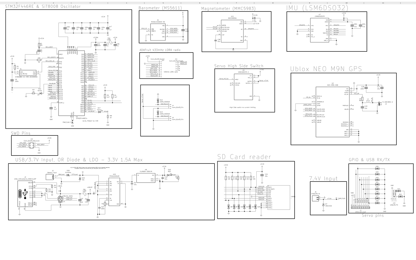
The sensor set is split across three buses so the fast inertial reads never queue behind a slow transfer, and every exposed connector gets its own protection at the pin.
Why these parts
The STM32F446RE was picked over an Arduino-class board for control and for visibility. Timers, interrupts, the data lines and DMA all get configured directly, and serial-wire debug gives breakpoints and live register inspection rather than print statements — which matters when the bug only shows up under flight timing. The large user base meant there was reference material whenever something did not work.
Four layers rather than two, in a signal / ground / power / signal stackup, so a continuous ground reference sits under every sensor trace. That plane is what keeps EMI and crosstalk off a noise-sensitive IMU and barometer, and the extra fabrication cost is simply the price of having it.
The servos run anywhere from 6 to 8.2 V. An early iteration used a buck-boost converter to reach 8.2 V for the extra torque, but running straight off the 7.4 V a 2S li-ion pack already provides gave adequate torque without the converter, so the converter came out.
An RTOS rather than a bare-metal super-loop, to enforce deterministic timing across concurrent tasks and to make adding or removing a feature a local change instead of a rework of the whole schedule.
50 Ω to the antenna
The u-blox NEO-M9N needs a 50 Ω feed. So does the U.FL connector and the coax running out to the antenna, so the trace between them had to be 50 Ω too.
The geometry was worked out in KiCad's PCB Calculator, under Transmission Lines. The trace has ground poured either side of it and a ground plane underneath, so it was solved as a coplanar waveguide with ground rather than a plain microstrip. These are the values that went in, and where each one came from.
| Field | Value | Where it came from |
|---|---|---|
| Er | 4.4 | JLCPCB's prepreg table for the 7628 layer between L1 and L2. |
| H | 0.2 mm | The L1-to-L2 dielectric height on the four-layer 1.6 mm stackup. |
| T | 0.035 mm | 1 oz outer copper, which is what was ordered. |
| Frequency | 1.575 GHz | GPS L1, so the calculator applies its dispersion correction. |
| Z0 | 50 Ω | What the NEO-M9N's RF input is designed for. |
The result
Synthesize gives back the two numbers that were actually needed: how wide to draw the trace, and how far to hold the ground pour off it. Measuring what had really been routed and typing it back in for Analyze solves the other direction, and reports the impedance of the trace as drawn.
A trace roughly 0.30 to 0.33 mm wide with a 0.25 mm gap to the ground pour either side. Running the routed geometry back through in Analyze mode puts it inside 50 ± 5 Ω, within the fabricator's tolerance. The feed has no vias and no stubs, an unbroken ground plane underneath, stitching vias every couple of millimetres along it, and 45° turns instead of square corners.
SDIO length matching
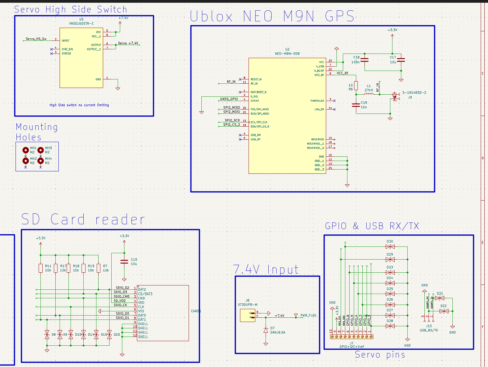
SDIO is the only source-synchronous parallel bus on the board. Clock, command and four data lines all get sampled against the same clock edge, so all six were length matched to within 2.5 mm of each other, on the same layer over the same reference plane, with the clock routed centrally in the group.
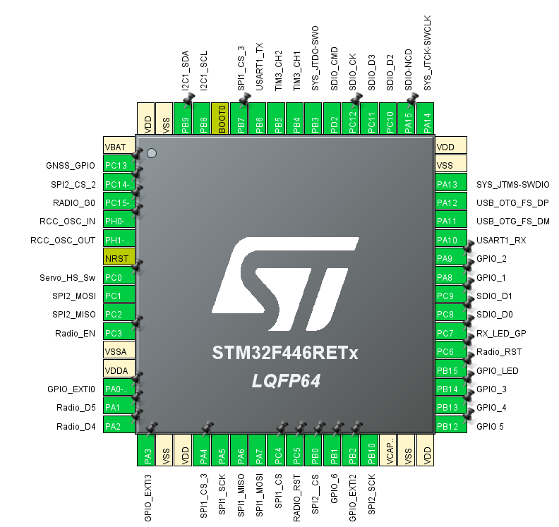
The constraint nobody expected came from reading the package pinout instead of the netlist. The SDIO signals do not all leave the chip on the same side: clock, command and two data lines come out the north edge, the other two come out the east. Two of the six matched nets have to go around a corner of the package before they even start heading for the socket, which builds a mismatch in before any routing happens. The socket was placed so both groups converge.
The oscillator and the GPS band
The same exercise turned up a second constraint. The oscillator pins come out the west edge — the same side the GPS receiver wants to sit on — and the oscillator's harmonics land in the GPS band.
The oscillator went at the far end of the west edge from the antenna port, with stitched ground poured between them.
Power
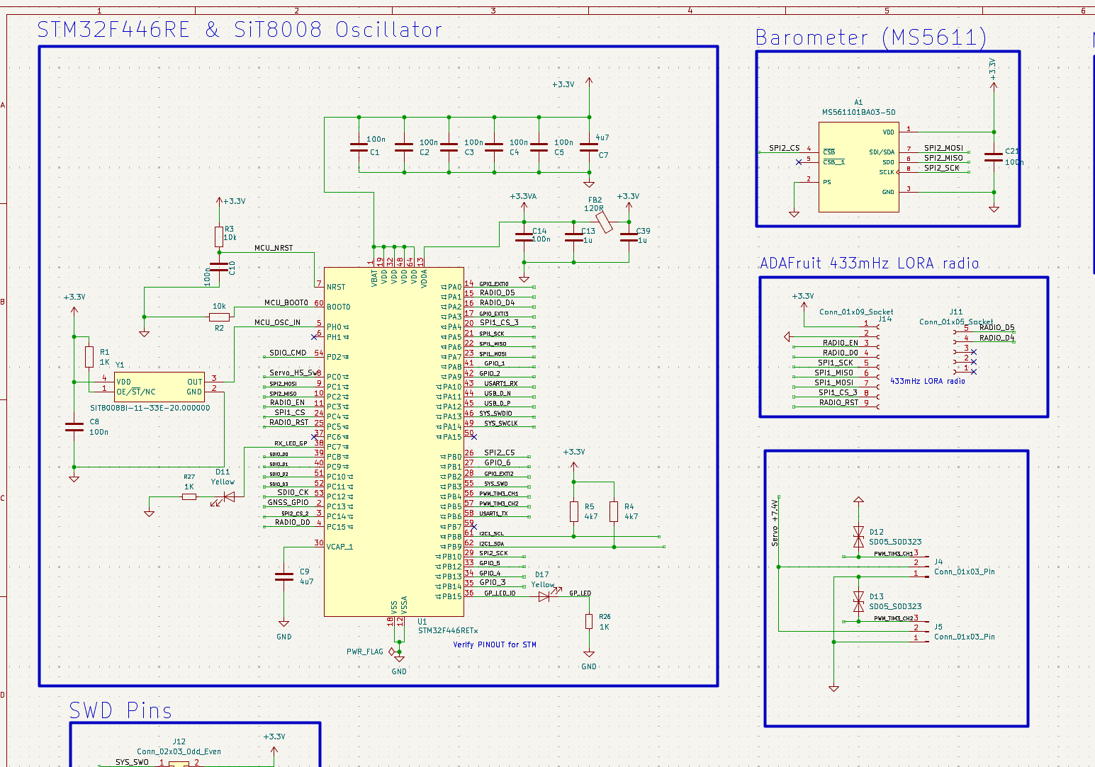
Two inputs, seamless changeover. USB-C with the CC pull-downs that make a source hand over power, plus a separate battery input taking 3.7 to 7.4 V through a Schottky and a TVS, with a TPS2121 priority mux swapping between them. The second input exists because competition rules require the tracking element to be powered independently.
A low-noise 3.3 V rail, from a TL1963A linear regulator rather than a switcher, so there are no switching harmonics landing in the GPS band. It gets copper area and thermal vias, and sits well away from the barometer.
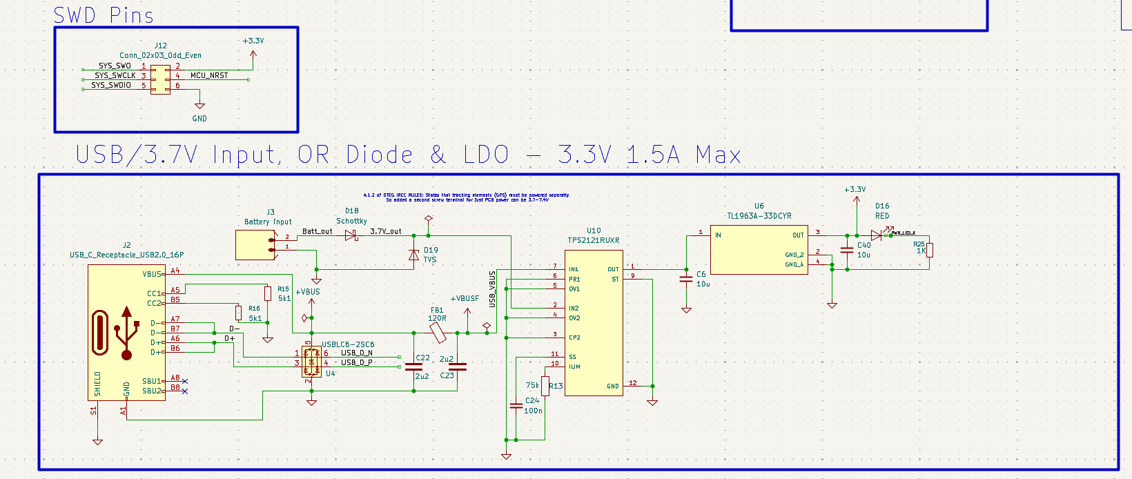
The servo rail is an island. A TVS clamps the spike from unplugging a loaded servo, and a VN5E160 high-side switch gates the rail under firmware control. It is poured as its own island at one board edge so its return current never crosses the sensor or RF ground. Everything exposed — the GPIO header, the UART header, the USB pair and the SD interface — gets ESD protection placed right at the connector.
What made it hard
Mixed-signal noise was the recurring one. The servo rail puts switching noise straight into the IMU if it shares a return path, which is why the ground plane is split at the power entry, the servo driver is ringed with stitching vias, and the sensor lines are routed away from the high-current traces.
The other was fitting everything inside the control-loop deadline. Polling sensors, running the estimator and logging to SD all compete for the same budget, so priority is assigned rather than left to chance: sensor polling and actuator commands sit at the top, and SD logging is deferred to a low-priority task behind a ring buffer so a slow write can never block the loop.
Bring-up and what's next
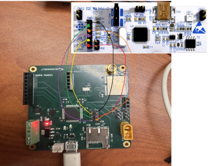
The board is built and running, brought up over SWD with an ST-Link. A new flight computer is in design for December: SDIO on a single package edge this time, and controlled-impedance routing planned out from the stackup at the start.